Introduction
Semiconductor wafers are fundamental to the semiconductor industry, serving as the substrate for integrated circuits (ICs) and various electronic components. The precision and quality of these wafers are critical for the performance and reliability of semiconductor devices. Machining plays a vital role in producing high-quality semiconductor wafers, ensuring they meet stringent specifications. This article explores the importance of semiconductor wafers, the machining processes involved in their production, and their applications in the semiconductor industry.
Understanding Semiconductor Wafers
Semiconductor wafers are thin slices of semiconductor material, typically silicon, used as the foundation for fabricating integrated circuits and other microdevices. These wafers undergo multiple processing steps, including doping, etching, and deposition, to create the intricate electronic circuits essential for modern electronic devices.
- Material:
- Silicon: The most commonly used material for semiconductor wafers due to its excellent electrical properties and abundance.
- Other Materials: Gallium arsenide (GaAs), silicon carbide (SiC), and indium phosphide (InP) are used for specialized applications requiring specific electronic properties.
- Dimensions:
- Diameter: Typically ranges from 100 mm (4 inches) to 300 mm (12 inches), with larger wafers enabling the production of more devices per wafer.
- Thickness: Varies based on the application and manufacturing process, with precise control required to ensure uniformity.
Machining Processes for Semiconductor Wafers
- Crystal Growth and Ingot Formation:
- Process: High-purity semiconductor material is melted and grown into a single crystal ingot using methods such as the Czochralski (CZ) process.
- Machining Role: Precision cutting of the ingot into cylindrical shapes, ensuring the crystal orientation is maintained.
- Wafer Slicing:
- Process: The ingot is sliced into thin wafers using wire saws or diamond-coated blades.
- Machining Role: Achieving uniform thickness and minimal kerf loss (material waste) during slicing.
- Edge Grinding:
- Process: The edges of the wafers are ground to a precise diameter and shape to prevent chipping and improve handling.
- Machining Role: Ensuring smooth, defect-free edges with tight dimensional tolerances.
- Lapping:
- Process: Wafers are lapped using abrasive slurry and a rotating lap to achieve flat, smooth surfaces.
- Machining Role: Removing saw marks and achieving the required flatness and parallelism.
- Polishing:
- Process: Fine abrasives and a polishing pad are used to achieve a mirror-like finish on the wafer surfaces.
- Machining Role: Producing ultra-smooth surfaces with low roughness values, essential for subsequent photolithography and etching processes.
- Chemical Mechanical Planarization (CMP):
- Process: Combines chemical and mechanical processes to planarize the wafer surface.
- Machining Role: Achieving a highly planar surface with minimal defects, critical for multi-layer device fabrication.
Benefits of Precision Machining for Semiconductor Wafers
- High Precision and Accuracy:
- Benefit: Machining processes can achieve extremely tight tolerances and high dimensional accuracy.
- Impact: Ensures that wafers meet the exacting specifications required for semiconductor manufacturing.
- Uniformity and Consistency:
- Benefit: Precision machining ensures uniform thickness and surface quality across all wafers.
- Impact: Reduces variability and defects, leading to higher yields and more reliable devices.
- Surface Quality:
- Benefit: Lapping, polishing, and CMP produce surfaces with very low roughness values and high optical clarity.
- Impact: Essential for high-resolution photolithography and defect-free device fabrication.
- Reduced Defects:
- Benefit: Machining processes help remove surface and subsurface defects, such as micro-cracks and dislocations.
- Impact: Minimizes the risk of device failure and improves the overall quality of semiconductor products.
- Scalability:
- Benefit: Advanced machining techniques can be scaled to accommodate larger wafer sizes and higher production volumes.
- Impact: Supports the growing demand for semiconductor devices in various applications.
Applications of Semiconductor Wafers
- Integrated Circuits (ICs):
- Description: Semiconductor wafers serve as the substrate for ICs, which are used in virtually all electronic devices.
- Application: Microprocessors, memory chips, and application-specific integrated circuits (ASICs).
- Microelectromechanical Systems (MEMS):
- Description: MEMS devices integrate mechanical and electrical components at a microscale.
- Application: Sensors, actuators, and microfluidic devices.
- Optoelectronics:
- Description: Devices that interact with light, such as LEDs, laser diodes, and photodetectors.
- Application: Displays, communication systems, and medical devices.
- Power Devices:
- Description: Semiconductor wafers are used to fabricate power electronic devices that manage and convert electrical power.
- Application: Power transistors, diodes, and thyristors used in power supplies and energy management systems.
- Solar Cells:
- Description: Semiconductor wafers, particularly silicon, are used to manufacture photovoltaic cells that convert sunlight into electricity.
- Application: Solar panels and renewable energy systems.
Conclusion
Semiconductor wafers are a crucial component in the semiconductor industry, serving as the foundation for a wide range of electronic devices. Precision machining processes such as slicing, edge grinding, lapping, polishing, and chemical mechanical planarization are essential for producing high-quality wafers that meet the stringent requirements of modern semiconductor manufacturing. As the demand for advanced and reliable semiconductor devices continues to grow, the importance of precision machining in the production of semiconductor wafers will remain paramount, driving innovation and excellence in the industry.
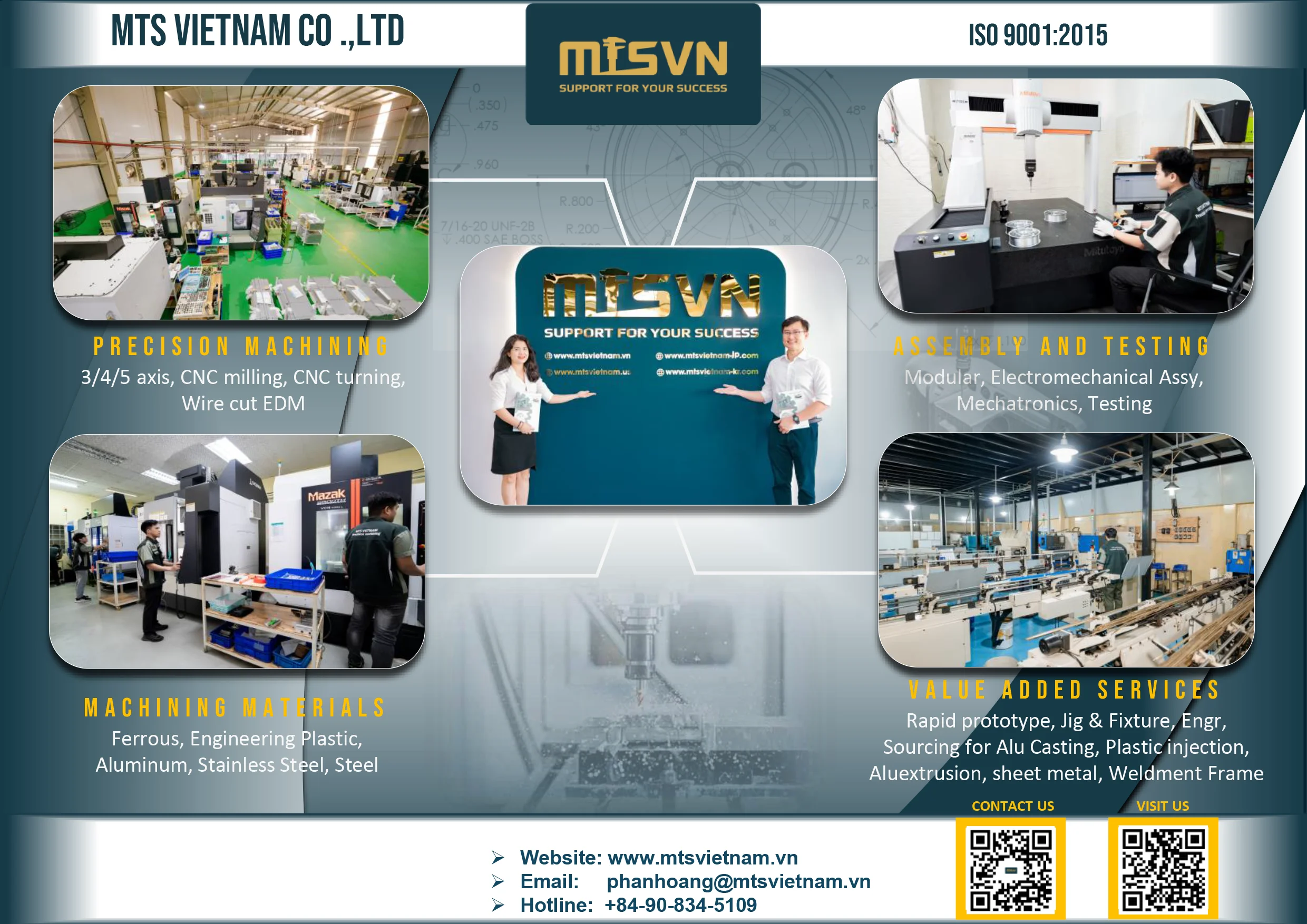
MTS Vietnam is a prominent company specializing in precision mechanical components fabrication. Established in 2017, it has quickly become a reputable name in the Vietnamese and Southeast Asian markets. The company's expertise lies in CNC milling and turning parts made from a variety of materials, including Aluminum, Steel, Stainless, POM, and other engineering plastics. MTS Vietnam is dedicated to supporting the success of its customers and strives to be a leading company in the field of precision mechanical processing both in Vietnam and internationally.
In addition to its fabrication services, MTS Vietnam offers assembly services for components and machines, as well as CNC program services. This comprehensive range of services is aimed at providing optimal solutions and benefits to its customers through the company's ecosystem and strengths. MTS Vietnam emphasizes the importance of investing in new technology and quality control equipment to ensure that it can deliver merchandise at competitive prices and within the required deadlines.
WORKSHOP: 248/10 ĐT743A Street, Binh Thung 1 Quarter, Dong Hoa Ward, Ho Chi Minh City, Vietnam
Tel/zalo/viber: 0908.345.109
Email: phanhoang@mtsvietnam.vn | info@mtsvietnam.vn
Website: www.mtsvietnam.vn (Global Market) | www.mtsvietnam-jp.com (日本)
For USA Sales, please contact MTS USA at:
Tel/zalo/viber: 978-777-1716
Email: sales@mts-usasales.com
Website: www.mtsvietnam.us (US Market)