Introduction
The semiconductor industry is essential for the advancement of modern electronics, enabling the production of sophisticated devices that power our world. Packaging and test equipment are critical components in this industry, ensuring that semiconductor devices are protected, reliable, and perform as expected. Precision machined parts play a vital role in the functionality and accuracy of packaging and test equipment. This article explores the importance of packaging and test equipment, the role of precision machining in their production, and their applications in the semiconductor industry.
Understanding Packaging and Test Equipment
Packaging and test equipment are essential for the final stages of semiconductor manufacturing. They ensure that semiconductor devices are properly encapsulated, protected, and tested for functionality and reliability before being shipped to customers.
- Packaging Equipment:
- Function: Encapsulates semiconductor devices in protective packages that shield them from physical damage, moisture, and contaminants.
- Types: Wire bonders, die attach machines, encapsulation systems, and packaging inspection systems.
- Test Equipment:
- Function: Tests semiconductor devices to ensure they meet specified performance and reliability standards.
- Types: Automated test equipment (ATE), probe stations, burn-in ovens, and reliability test systems.
Importance of Precision Machining in Packaging and Test Equipment
- High Precision and Accuracy:
- Benefit: Precision machined parts ensure that packaging and test equipment can achieve the extremely tight tolerances required for handling and testing semiconductor devices.
- Impact: Ensures accurate placement, bonding, and testing of semiconductor devices, leading to higher quality and reliability.
- Complex Geometries:
- Benefit: Many components of packaging and test equipment have intricate shapes and fine features that require advanced machining techniques.
- Impact: Supports the development of sophisticated systems and mechanisms within the equipment.
- Material Properties:
- Benefit: Components must be made from materials with specific properties, such as thermal stability, electrical conductivity, and resistance to wear.
- Impact: Ensures the reliability and longevity of packaging and test equipment under demanding manufacturing conditions.
- Consistency and Repeatability:
- Benefit: Precision machining provides consistent and repeatable results, producing identical parts across large production runs.
- Impact: Reduces variability and defects, ensuring uniform performance of packaging and test equipment.
- Surface Finish Quality:
- Benefit: High-quality surface finishes are essential for components that interact with semiconductor devices to reduce friction and improve handling precision.
- Impact: Enhances the performance and reliability of the packaging and testing processes.
Applications of Machined Parts in Packaging and Test Equipment
- Wire Bonders:
- Description: Machines that connect semiconductor die to package leads using fine wires.
- Machining Role: Producing precision components such as bonding heads, capillaries, and clamps to ensure accurate and reliable wire bonding.
- Die Attach Machines:
- Description: Equipment that attaches semiconductor die to substrates or packages using adhesives or solder.
- Machining Role: Creating precise placement mechanisms and dispensing systems for accurate die attachment.
- Encapsulation Systems:
- Description: Systems that encapsulate semiconductor devices in protective materials, such as epoxy or plastic.
- Machining Role: Manufacturing molds, nozzles, and dispensing heads with tight tolerances to ensure uniform encapsulation.
- Automated Test Equipment (ATE):
- Description: Systems that automatically test the functionality and performance of semiconductor devices.
- Machining Role: Producing high-precision test sockets, probes, and contactors that ensure accurate and reliable testing.
- Probe Stations:
- Description: Equipment used to test semiconductor wafers at the wafer level before they are diced into individual chips.
- Machining Role: Manufacturing precise probes, stages, and alignment systems for accurate wafer testing.
- Burn-In Ovens:
- Description: Ovens used to stress semiconductor devices by exposing them to elevated temperatures and electrical loads.
- Machining Role: Creating high-precision heating elements, fixtures, and enclosures to ensure consistent and reliable burn-in testing.
Challenges and Solutions in Machining Parts for Packaging and Test Equipment
- Maintaining Tight Tolerances:
- Challenge: Achieving the extremely tight tolerances required for equipment components.
- Solution: Utilizing advanced CNC machining techniques, high-precision tooling, and rigorous quality control measures.
- Surface Finish Requirements:
- Challenge: Ensuring high-quality surface finishes for components that interact with semiconductor devices.
- Solution: Employing fine-grit abrasives, polishing processes, and precision lapping techniques to achieve the desired finish.
- Material Selection and Machining:
- Challenge: Machining materials with specific properties, such as thermal stability and electrical conductivity.
- Solution: Selecting appropriate materials and optimizing machining parameters to maintain material properties while achieving high precision.
- Component Complexity:
- Challenge: Machining complex geometries and fine features required for advanced equipment.
- Solution: Using multi-axis CNC machines, advanced CAD/CAM software, and skilled machinists to produce intricate parts.
Conclusion
Packaging and test equipment are crucial components of the semiconductor manufacturing process, ensuring that semiconductor devices are protected, reliable, and meet performance standards. The production of high-quality packaging and test equipment relies heavily on precision machining to achieve the required accuracy, consistency, and surface finish. By supporting the creation of intricate wire bonders, die attach machines, encapsulation systems, and automated test equipment, precision machining plays an indispensable role in the semiconductor industry. As technology advances and the demand for more sophisticated semiconductor devices grows, the importance of precision machining in the development and production of packaging and test equipment will continue to be paramount.
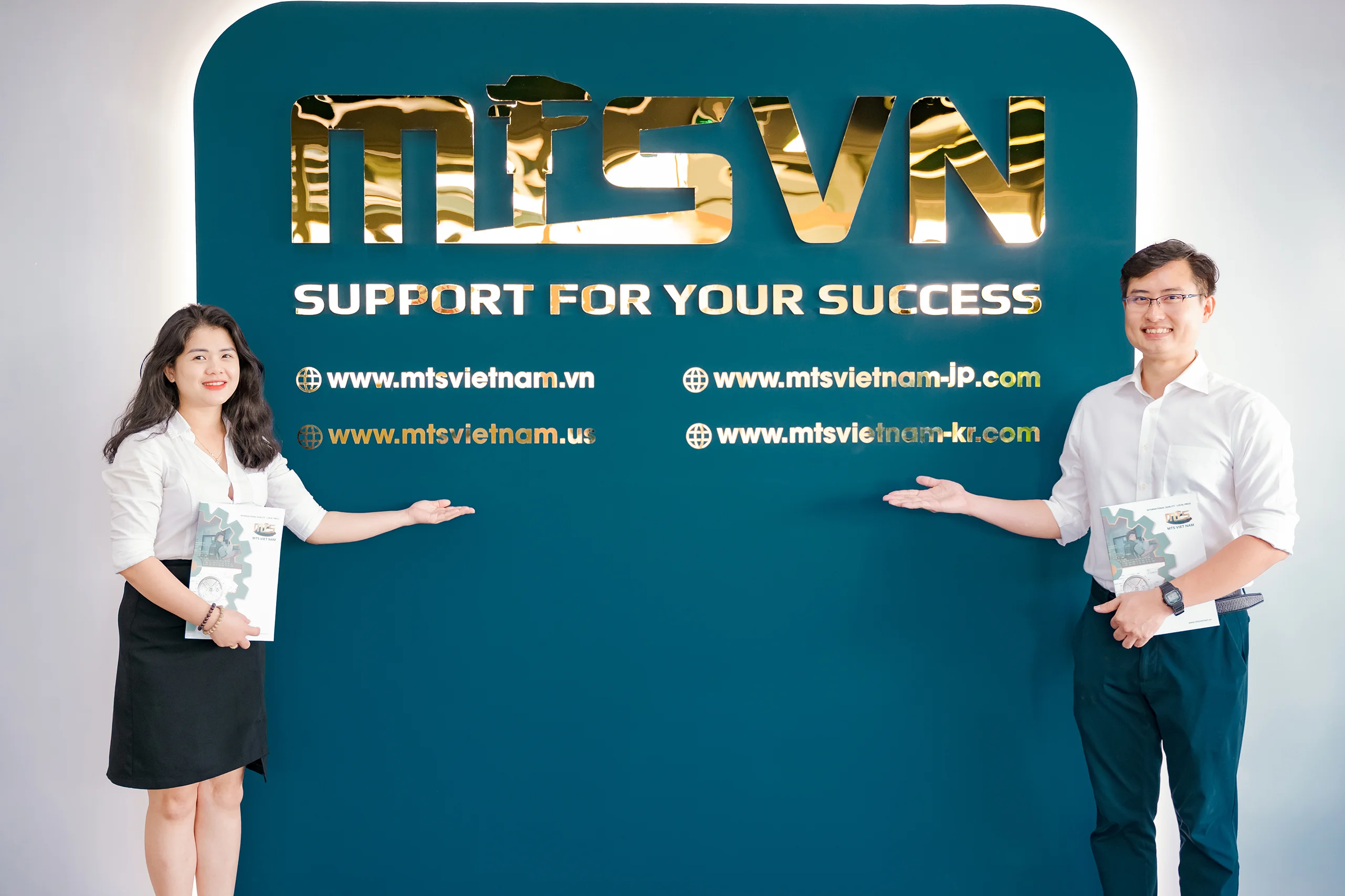
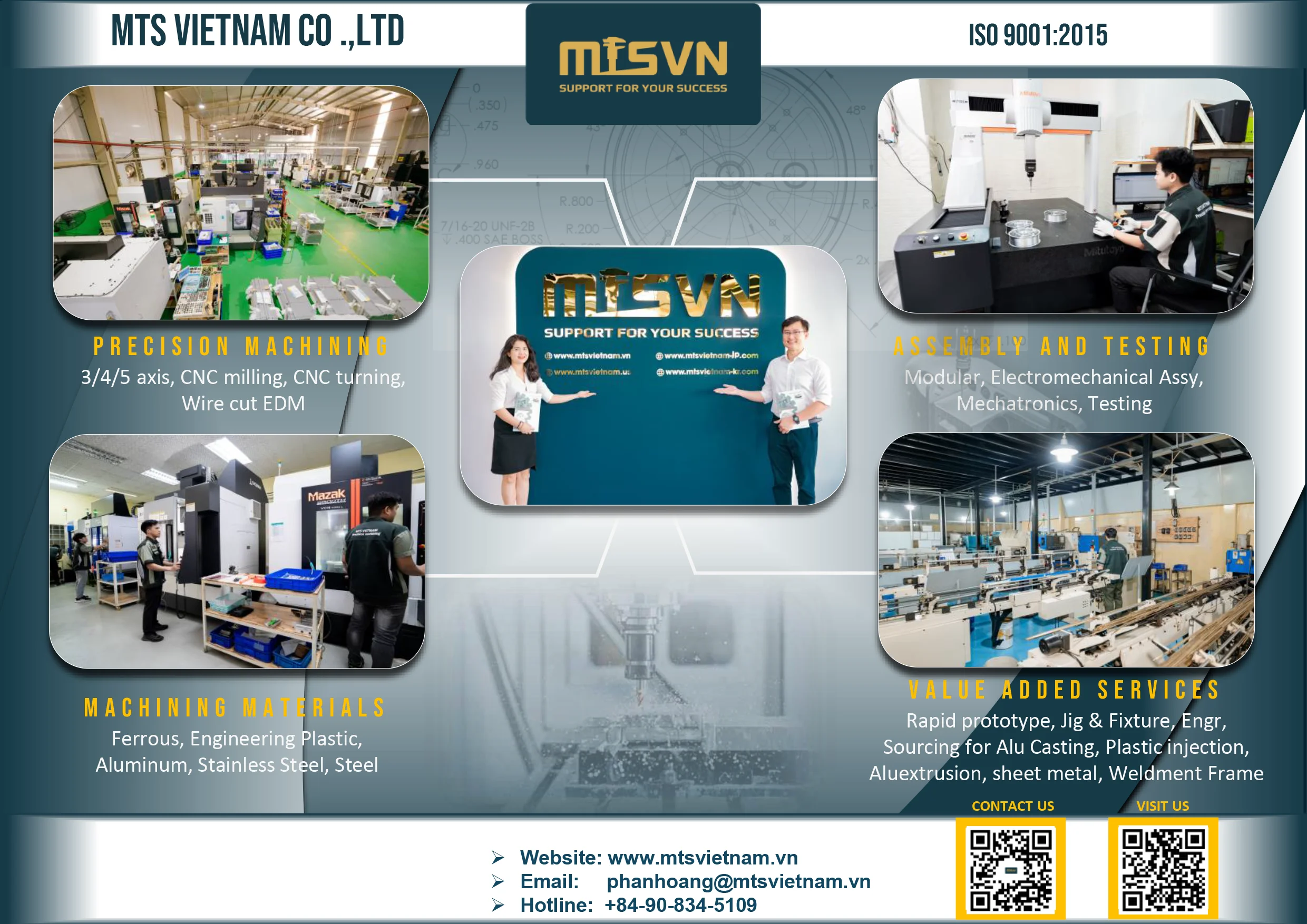
MTS Vietnam is a prominent company specializing in precision mechanical components fabrication. Established in 2017, it has quickly become a reputable name in the Vietnamese and Southeast Asian markets. The company's expertise lies in CNC milling and turning parts made from a variety of materials, including Aluminum, Steel, Stainless, POM, and other engineering plastics. MTS Vietnam is dedicated to supporting the success of its customers and strives to be a leading company in the field of precision mechanical processing both in Vietnam and internationally.
In addition to its fabrication services, MTS Vietnam offers assembly services for components and machines, as well as CNC program services. This comprehensive range of services is aimed at providing optimal solutions and benefits to its customers through the company's ecosystem and strengths. MTS Vietnam emphasizes the importance of investing in new technology and quality control equipment to ensure that it can deliver merchandise at competitive prices and within the required deadlines.
WORKSHOP: 248/10 ĐT743A Street, Binh Thung 1 Quarter, Dong Hoa Ward, Ho Chi Minh City, Vietnam
Tel/zalo/viber: 0908.345.109
Email: phanhoang@mtsvietnam.vn | info@mtsvietnam.vn
Website: www.mtsvietnam.vn (Global Market) | www.mtsvietnam-jp.com (日本)
For USA Sales, please contact MTS USA at:
Tel/zalo/viber: 978-777-1716
Email: sales@mts-usasales.com
Website: www.mtsvietnam.us (US Market)