Introduction
The semiconductor industry is foundational to the development of modern electronics, requiring highly precise and flawless components. Among the key machining techniques that ensure the high quality of these components are lapping and polishing. These processes are essential for achieving the ultra-smooth surfaces and tight tolerances required in semiconductor manufacturing. This article explores the role of lapping and polishing in the semiconductor industry, their benefits, applications, and why they are considered indispensable techniques.
Understanding Lapping and Polishing
Lapping and polishing are abrasive machining processes used to achieve high levels of surface finish and dimensional accuracy. While both processes aim to produce smooth and flat surfaces, they differ in their mechanisms and applications.
- Lapping:
- Process: Lapping involves the use of a rotating lap (a flat surface) and abrasive slurry to remove material from a workpiece. The workpiece is pressed against the lap and moved in a controlled manner to achieve a flat, smooth surface.
- Materials: Typically used on metals, ceramics, and semiconductor materials such as silicon and gallium arsenide.
- Outcomes: Produces very flat surfaces with minimal material removal, ideal for preparing surfaces for further processing.
- Polishing:
- Process: Polishing uses fine abrasive particles and a rotating polishing pad to smooth the surface of a workpiece. The process is similar to lapping but generally uses finer abrasives and less pressure.
- Materials: Applied to metals, ceramics, glass, and semiconductor materials.
- Outcomes: Achieves ultra-smooth surfaces with a mirror-like finish, essential for optical and electronic components.
Benefits of Lapping and Polishing in the Semiconductor Industry
- High Precision and Accuracy:
- Benefit: Both lapping and polishing can achieve extremely tight tolerances and high dimensional accuracy.
- Impact: Ensures that semiconductor components meet the stringent specifications required for optimal performance and reliability.
- Ultra-Smooth Surfaces:
- Benefit: These processes can produce surfaces with very low roughness values, often in the nanometer range.
- Impact: Essential for reducing defects, improving optical clarity, and enhancing electrical properties of semiconductor devices.
- Improved Performance:
- Benefit: Smooth and flat surfaces improve the performance and efficiency of semiconductor components by reducing friction, enhancing thermal conductivity, and ensuring better electrical contacts.
- Impact: Leads to more reliable and efficient semiconductor devices.
- Defect Reduction:
- Benefit: Lapping and polishing help to remove surface defects such as scratches, pits, and contamination.
- Impact: Minimizes the risk of device failure and increases the yield of semiconductor manufacturing processes.
- Compatibility with Multiple Materials:
- Benefit: These techniques can be applied to a wide range of materials used in semiconductor manufacturing, including silicon, sapphire, and various ceramics.
- Impact: Provides versatility in processing different types of semiconductor components.
Applications of Lapping and Polishing in the Semiconductor Industry
- Semiconductor Wafers:
- Description: Thin slices of semiconductor material used as the substrate for integrated circuits and other devices.
- Lapping and Polishing Role: Achieves the required flatness, smoothness, and thickness uniformity necessary for subsequent photolithography and etching processes.
- Optical Components:
- Description: Lenses, mirrors, and other optical elements used in semiconductor equipment.
- Lapping and Polishing Role: Produces surfaces with high optical clarity and precision, essential for accurate light manipulation.
- Microelectromechanical Systems (MEMS):
- Description: Devices that integrate mechanical and electrical components at a microscale.
- Lapping and Polishing Role: Ensures flat and smooth surfaces for precise mechanical movement and reliable electrical connections.
- Integrated Circuits (ICs):
- Description: Chips that house multiple electronic components interconnected to perform complex functions.
- Lapping and Polishing Role: Prepares the surfaces of wafers and IC packages to ensure optimal adhesion, bonding, and functionality.
- Ceramic Substrates:
- Description: Insulating materials used to support and connect electronic components.
- Lapping and Polishing Role: Produces flat, smooth surfaces for reliable mounting and interconnection of electronic components.
Challenges and Solutions in Lapping and Polishing for the Semiconductor Industry
- Maintaining Consistency:
- Challenge: Achieving consistent surface quality across large batches.
- Solution: Implementing strict process controls, using high-quality abrasives, and employing automated systems to ensure uniformity.
- Contamination Control:
- Challenge: Preventing contamination of the workpiece during processing.
- Solution: Utilizing cleanroom environments, high-purity abrasives, and thorough cleaning protocols to maintain surface purity.
- Process Optimization:
- Challenge: Balancing material removal rates with surface quality.
- Solution: Fine-tuning process parameters, such as pressure, speed, and abrasive size, to optimize the balance between efficiency and quality.
- Tool Wear:
- Challenge: Managing the wear of lapping and polishing tools.
- Solution: Regular monitoring and maintenance of tools, along with the use of wear-resistant materials, to maintain precision and performance.
Conclusion
Lapping and polishing are key machining techniques in the semiconductor industry, providing the precision, accuracy, and surface quality necessary for high-performance semiconductor components. These processes ensure that semiconductor wafers, optical components, MEMS devices, integrated circuits, and ceramic substrates meet the stringent standards required for modern electronics. As the demand for more advanced and reliable semiconductor devices continues to grow, lapping and polishing will remain indispensable processes, driving innovation and excellence in the semiconductor industry.
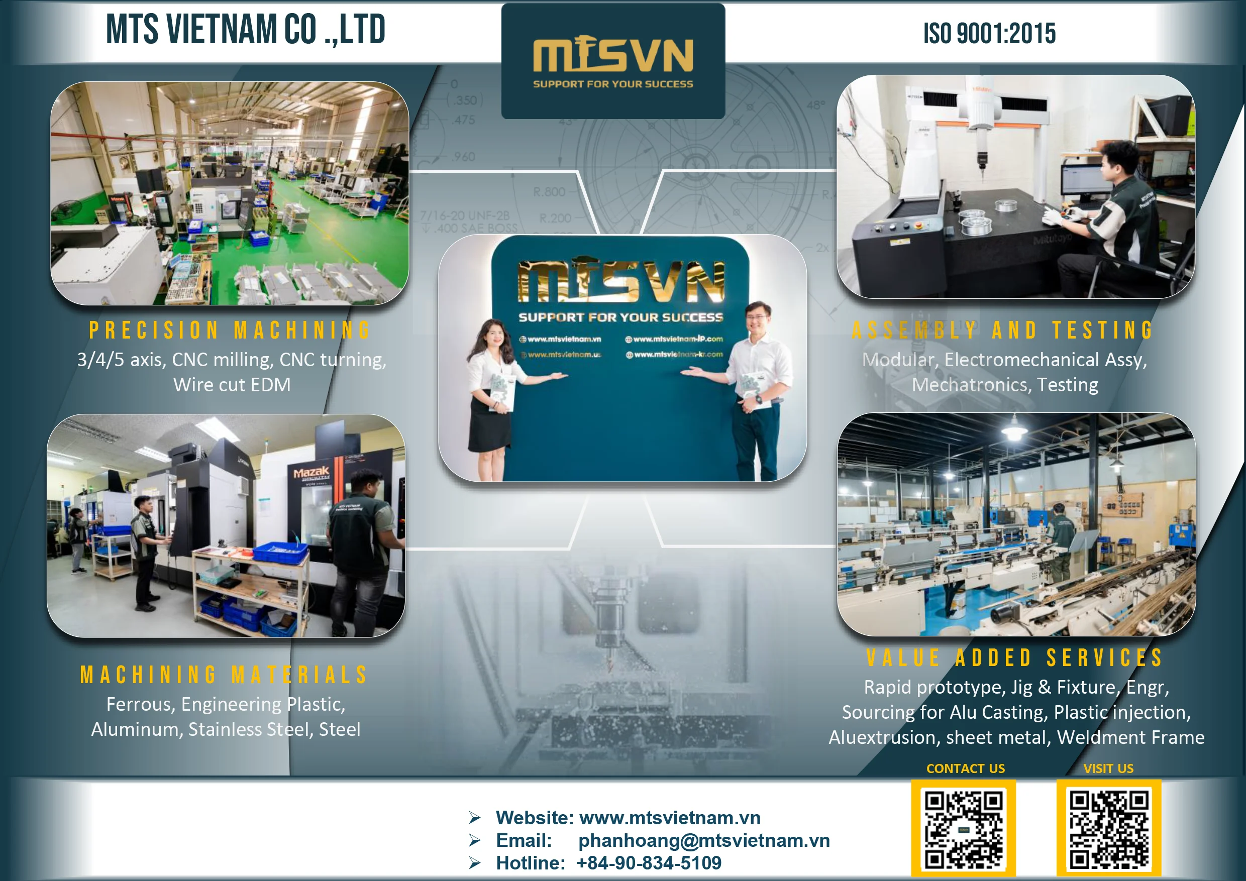
MTS Vietnam is a prominent company specializing in precision mechanical components fabrication. Established in 2017, it has quickly become a reputable name in the Vietnamese and Southeast Asian markets. The company's expertise lies in CNC milling and turning parts made from a variety of materials, including Aluminum, Steel, Stainless, POM, and other engineering plastics. MTS Vietnam is dedicated to supporting the success of its customers and strives to be a leading company in the field of precision mechanical processing both in Vietnam and internationally.
In addition to its fabrication services, MTS Vietnam offers assembly services for components and machines, as well as CNC program services. This comprehensive range of services is aimed at providing optimal solutions and benefits to its customers through the company's ecosystem and strengths. MTS Vietnam emphasizes the importance of investing in new technology and quality control equipment to ensure that it can deliver merchandise at competitive prices and within the required deadlines.
WORKSHOP: 248/10 ĐT743A Street, Binh Thung 1 Quarter, Dong Hoa Ward, Ho Chi Minh City, Vietnam
Tel/zalo/viber: 0908.345.109
Email: phanhoang@mtsvietnam.vn | info@mtsvietnam.vn
Website: www.mtsvietnam.vn (Global Market) | www.mtsvietnam-jp.com (日本)
For USA Sales, please contact MTS USA at:
Tel/zalo/viber: 978-777-1716
Email: sales@mts-usasales.com
Website: www.mtsvietnam.us (US Market)