Introduction
The semiconductor industry is fundamental to the advancement of modern technology, necessitating highly precise and intricate components. One of the crucial machining techniques employed to achieve such precision is Electrical Discharge Machining (EDM). EDM is particularly valued for its ability to machine complex geometries and hard materials with exceptional accuracy. This article delves into the role of EDM in the semiconductor industry, its benefits, applications, and why it stands out as a key machining technique.
Understanding EDM
Electrical Discharge Machining (EDM) is a non-traditional machining process that uses electrical discharges (sparks) to erode material from a workpiece. This technique is especially effective for machining hard materials and creating intricate shapes that would be challenging or impossible to achieve with conventional machining methods.
- How EDM Works:
- Setup: The EDM process involves two main components: the electrode (usually made of graphite or copper) and the workpiece. Both are submerged in a dielectric fluid, typically deionized water or oil.
- Operation: A series of electrical discharges occur between the electrode and the workpiece, controlled by a power supply. These discharges generate intense heat, which melts and vaporizes small amounts of the workpiece material.
- Material Removal: The dielectric fluid flushes away the eroded particles, cools the work area, and prevents short circuits by acting as an insulator.
- Types of EDM:
- Wire EDM: Uses a thin, electrically charged wire as the electrode to cut through the workpiece, ideal for producing complex shapes and fine details.
- Sinker EDM: Uses a shaped electrode that is plunged into the workpiece, suitable for creating cavities, molds, and intricate 3D shapes.
Benefits of EDM in the Semiconductor Industry
- Machining Hard Materials:
- Benefit: EDM can machine materials that are difficult or impossible to cut with traditional methods, such as hardened steel, tungsten carbide, and conductive ceramics.
- Impact: Enables the production of durable and high-performance semiconductor components.
- Complex Geometries:
- Benefit: EDM can produce intricate shapes, fine details, and tight corners with high precision.
- Impact: Essential for creating the complex geometries required in semiconductor devices, such as microelectromechanical systems (MEMS) and integrated circuits (ICs)
- Precision and Accuracy:
- Benefit: EDM offers exceptional precision and accuracy, capable of achieving tolerances within a few microns.
- Impact: Ensures that semiconductor components meet the stringent specifications necessary for optimal performance and reliability.
- No Mechanical Stress:
- Benefit: EDM is a non-contact machining process, which means there is no physical force applied to the workpiece.
- Impact: Prevents deformation and damage, preserving the integrity of delicate and fragile components.
- Surface Finish:
- Benefit: EDM can achieve excellent surface finishes, often eliminating the need for additional polishing or finishing processes.
- Impact: Enhances the quality and performance of semiconductor components by reducing friction and wear.
Applications of EDM in the Semiconductor Industry
- Microelectromechanical Systems (MEMS):
- Description: MEMS devices consist of tiny mechanical components that interact with electronic circuits.
- EDM Role: Produces intricate and precise features, such as micro-gears, micro-sensors, and micro-actuators.
- Integrated Circuits (ICs):
- Description: ICs are the building blocks of modern electronic devices, containing multiple interconnected electronic components.
- EDM Role: Machines the fine details and complex structures required for IC molds and dies.
- Semiconductor Wafers:
- Description: Thin slices of semiconductor material used as the substrate for ICs and other semiconductor devices.
- EDM Role: Precision cutting and shaping of wafers to ensure uniform thickness and smooth edges.
- Etching and Deposition Equipment:
- Description: Equipment used to create microstructures on semiconductor wafers through etching and deposition processes.
- EDM Role: Manufactures high-precision components, such as nozzles, chambers, and electrodes, which are critical for process accuracy.
- Molds and Dies for Semiconductor Packaging:
- Description: Molds and dies are used to shape and encapsulate semiconductor devices.
- EDM Role: Produces complex mold cavities and detailed features with high precision, ensuring the quality and reliability of semiconductor packages.
Challenges and Solutions in EDM for the Semiconductor Industry
- Material Removal Rate:
- Challenge: EDM can be slower compared to conventional machining methods.
- Solution: Optimization of EDM parameters, such as discharge energy, pulse duration, and dielectric fluid, can improve material removal rates.
- Electrode Wear:
- Challenge: The electrode in EDM can wear down over time, affecting precision and accuracy.
- Solution: Using high-quality electrode materials and optimizing machining parameters can reduce electrode wear and maintain accuracy.
- Thermal Effects:
- Challenge: The intense heat generated by EDM can cause thermal damage to the workpiece.
- Solution: Proper management of dielectric fluid and control of discharge parameters can minimize thermal effects and prevent damage.
- Surface Integrity:
- Challenge: EDM can sometimes leave a recast layer or micro-cracks on the machined surface.
- Solution: Post-processing techniques, such as polishing and surface treatments, can improve surface integrity and eliminate defects.
Conclusion
Electrical Discharge Machining (EDM) is a key machining technique in the semiconductor industry, offering unparalleled precision, accuracy, and the ability to machine complex geometries and hard materials. Its non-contact nature and exceptional surface finish capabilities make it indispensable for producing high-quality semiconductor components. As the demand for more advanced and miniaturized semiconductor devices continues to grow, EDM will remain a critical process, driving innovation and excellence in the semiconductor industry.
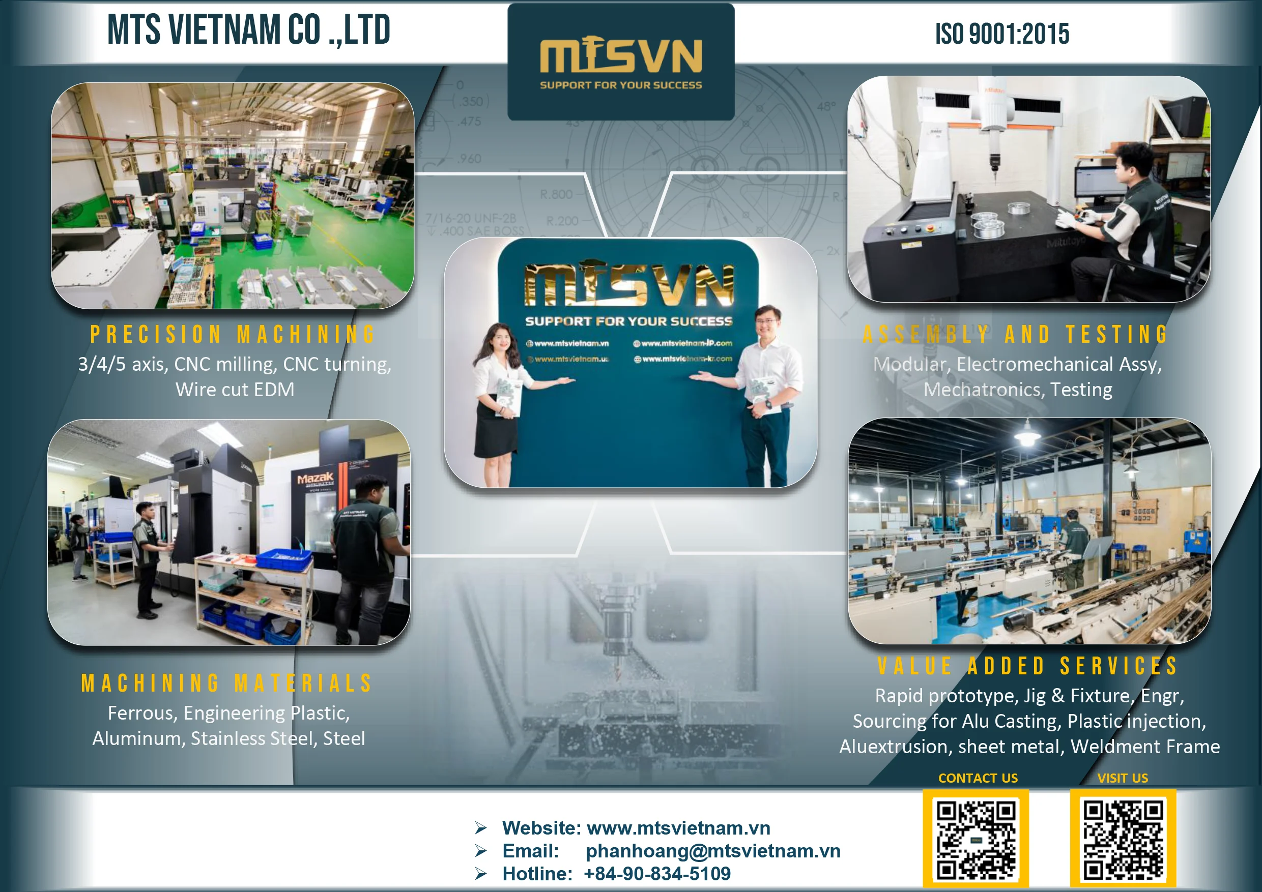
MTS Vietnam is a prominent company specializing in precision mechanical components fabrication. Established in 2017, it has quickly become a reputable name in the Vietnamese and Southeast Asian markets. The company's expertise lies in CNC milling and turning parts made from a variety of materials, including Aluminum, Steel, Stainless, POM, and other engineering plastics. MTS Vietnam is dedicated to supporting the success of its customers and strives to be a leading company in the field of precision mechanical processing both in Vietnam and internationally.
In addition to its fabrication services, MTS Vietnam offers assembly services for components and machines, as well as CNC program services. This comprehensive range of services is aimed at providing optimal solutions and benefits to its customers through the company's ecosystem and strengths. MTS Vietnam emphasizes the importance of investing in new technology and quality control equipment to ensure that it can deliver merchandise at competitive prices and within the required deadlines.
WORKSHOP: 248/10 ĐT743A Street, Binh Thung 1 Quarter, Dong Hoa Ward, Ho Chi Minh City, Vietnam
Tel/zalo/viber: 0908.345.109
Email: phanhoang@mtsvietnam.vn | info@mtsvietnam.vn
Website: www.mtsvietnam.vn (Global Market) | www.mtsvietnam-jp.com (日本)
For USA Sales, please contact MTS USA at:
Tel/zalo/viber: 978-777-1716
Email: sales@mts-usasales.com
Website: www.mtsvietnam.us (US Market)